Practical 3a - Vitis HLS Introduction
Task
Like at the start of practical 1a, this will be a bit of a tutorial to get you started with Vitis HLS. Go through this tutorial to make sure that you can get things working.
You will find the Vitis HLS knowledge base useful as it contains tips and reminders. There are some descriptions of common bug fixes there.
Until now, we have been using IP cores that were already provided for us. Now we will see how to use a high-level synthesis language to create our own. The tool we will use is called Vitis HLS, henceforth HLS (High-Level Synthesis). HLS takes C and C++ descriptions and converts them into a custom hardware IP core that we can use inside our Vivado projects.
Quick Recap
It is worth reviewing what the tools are and what they do:
Vivado
- Creates hardware designs (the bitfile) which describe what the reconfigurable hardware should do.
- Bolts together IP cores to make a complete design.
- Can be used to configure the FPGA (put a bitfile into the FPGA)
Vitis
- Software Development Environment
- Develops software for the processors of your design. In this course we focus only on developing software for the ARM cores.
- Can be used to configure the FPGA (put a bitfile into the FPGA) and also to put a compiled binary into memory for the ARM cores to run.
Vitis HLS
- Creates custom IP cores for you to use in Vivado.
Info
Vitis HLS used to be an entirely separate application to Vitis - but now it just a different “mode” in the main Vitis application.
Getting started with Vitis HLS
To create a new HLS project:
- Open Vitis, and go to your workspace.
- Select
File -> New Component -> HLS. - You can accept the name
hls_componentthis time but generally you should give it a descriptive name. Click Next. - On the Configuration File screen, click next.
- On the Add Source Files screen, click next.
- Select the Part to
xc7z010clg400-1. click next. - On the Edit Settings screen, click next, then Finish.
You are now looking at an HLS project, but it is empty. Create two new source files called toplevel.cpp and toplevel.h by right clicking the Sources folder in your project and selecting New Source File. Paste in the code below.
toplevel.cpp
#include "toplevel.h"

// Input data storage
#define NUMDATA 100

uint32 inputdata[NUMDATA];

//Prototypes
uint32 addall(uint32 * data);
uint32 subfromfirst(uint32 * data);

uint32 toplevel(uint32 * ram, uint32 * arg1, uint32 * arg2, uint32 * arg3, uint32 * arg4) {
#pragma HLS INTERFACE m_axi port=ram offset=slave bundle=MAXI
#pragma HLS INTERFACE s_axilite port=arg1 bundle=AXILiteS
#pragma HLS INTERFACE s_axilite port=arg2 bundle=AXILiteS
#pragma HLS INTERFACE s_axilite port=arg3 bundle=AXILiteS
#pragma HLS INTERFACE s_axilite port=arg4 bundle=AXILiteS
#pragma HLS INTERFACE s_axilite port=return bundle=AXILiteS

readloop:for (int i = 0; i < NUMDATA; i++) {
#pragma HLS PIPELINE off
		inputdata[i] = ram[i];
	}

	*arg2 = addall(inputdata);
	*arg3 = subfromfirst(inputdata);

	return *arg1 + 1;
}

uint32 addall(uint32 * data)
{
	uint32 total = 0;
	addloop: for (int i = 0; i < NUMDATA; i++) {
#pragma HLS PIPELINE off
		total = total + data[i];
	}
	return total;
}

uint32 subfromfirst(uint32 * data) {
	uint32 total = data[0];
	subloop: for (int i = 1; i < NUMDATA; i++) {
#pragma HLS PIPELINE off
		total = total - data[i];
	}
	return total;
}
toplevel.h
#ifndef __TOPLEVEL_H_
#define __TOPLEVEL_H_

#include <stdio.h>
#include <stdlib.h>
#include <ap_int.h>

//Typedefs
typedef unsigned int uint32;
typedef int int32;

uint32 toplevel(uint32 *ram, uint32 *arg1, uint32 *arg2, uint32 *arg3, uint32 *arg4);

#endif
Examine the Files
toplevel.cpp contains the structure that we will use throughout EMBS. The toplevel function has five arguments of type uint32. This is a typedef in toplevel.h that describes an unsigned integer of width 32 bits.
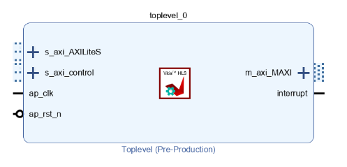
The file also contains pragmas which are called directives by HLS. Directives are used to tell HLS how to make your hardware. The directives here tell HLS to create an AXI Master interface, and AXI Slave interfaces. This is all described in the knowledge base. The Master interface allows the component to access main memory, and the slave interface allows the ARM cores to pass in a few variables and to start, reset, and stop the component. Once built and exported, your component will look like this in Vivado:
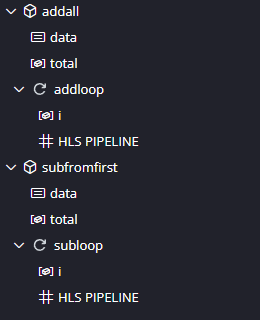
The file also contains our functionality. Note three important things:
- There is no
mainfunction. - We have declared a function
toplevel. This will be the ’entry point’ of the hardware. - The loops in the code have been given labels (
readloop,addloopandsubloop). Most programmers don’t do this, but it is useful in HLS, as you will see later.
Set the top level function
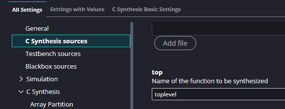
We need to tell HLS which function is the top level. In your hls_component, go to Settings -> hls_config.cfg and under C Synthesis sources find top and type in toplevel.
Testing Components
The last practicals showed you just how long hardware synthesis takes. You should therefore be pretty confident that your hardware is correct before building it. A testbench is an important part of this. Testbenches test the functional properties of the code, to make sure that it doesn’t contain any logical errors and it does roughly what you want. Testbenches cannot test how fast the final hardware will be because it is simulated in software.
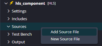
In HLS, right click ‘Test Bench’ in the Explorer on the left and select New Test Bench File. Call it testbench.cpp, and copy in the following code:testbench.cpp
#include "toplevel.h"
#define NUMDATA 100

uint32 mainmemory[NUMDATA];

int main() {

    //Create input data
    for(int i = 0; i < NUMDATA; i++) {
    	mainmemory[i] = i;
    }
    mainmemory[0] = 8000;

    //Set up the slave inputs to the hardware
    uint32 arg1 = 0;
    uint32 arg2 = 0;
    uint32 arg3 = 0;
    uint32 arg4 = 0;

    //Run the hardware
    toplevel(mainmemory, &arg1, &arg2, &arg3, &arg4);

    //Read the slave outputs
    printf("Sum of input: %d\n", arg2);
    printf("Values 1 to %d subtracted from value 0: %d\n", NUMDATA-1, arg3);

    //Check the values are as expected
    if(arg2 == 12950 && arg3 == 3050) {
        return 0;
    } else {
        return 1; //An error!
    }
}
Things to note:
- We declared a block of memory as “main memory”. In the real system this will be the 1GB of DDR memory on the Zybo Z7 board, but for the testbench we simply allocate an array that is large enough for our purposes.
- The testbench should return 0 if everything is OK. It checks the values returned from the hardware against pre-calculated values to ensure all is correct.
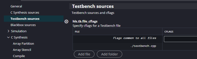
Before we can run the testbench we have to set it as a valid test bench. “But hang on!” I hear you ask. “Didn’t we already add it into a folder called Test Bench?” Well yes we did, but Xilinx. Anyway, go to Settings -> hls_config.cfg -> Testbench Sources and Add File to add it.
To run the testbench, in the Flow panel select C Simulation | Run and click Run in the dialog that appears. You should see HLS do quite a bit of work, but eventually you will see the output of the testbench.
Sum of input: 12950
Values 1 to 99 subtracted from value 0: 3050
@I [SIM-1] CSim done with 0 errors
We have verified our design. (You should probably test a real design a bit more rigorously!)
High-level synthesis
First, read the Important Terms You Should Know section of the Vitis HLS Knowledge Base. These are important terms and you should know them.
In the Flow panel click C Synthesis | Run. This will begin synthesis. Synthesis is the process of turning the C++ description into hardware. There are usually many different ways of achieving the same thing in hardware, all with different costs. HLS lets you explore these tradeoffs by applying directives.
If synthesis completed successfully, the Output log should show:
Synthesis finished successfully, open report.To view the synthesis report you can ctrl/cmd click the open report link in the log, or select from the Flow window C Synthesis -> Reports -> Synthesis. This report tells you all about the design that you’ve just built. Under Timing Estimate you will see the fastest estimated clock speed that this design could handle. When we created this project, we accepted the default clock frequency of 100 MHz which corresponds to a target clock period of 10 ns. The estimated fastest possible clock period should be around 7.3 ns so therefore we have met our target of 10 ns and so our design has “met timing closure”.
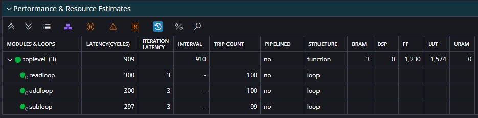
Now look at the Performance and Resource Estimates section. This tells you that your design has an overall latency (time from first data in to last data out) of 910 clock cycles. Its interval is 910 which is the amount of cycles from first data in of one run to the design being able to accept the first data in of another run.
Below the toplevel line it shows the three loops in the code (and this why it is useful to give them labels). A loop’s latency is the number of cycles it will take to complete. Sometimes HLS will not know this (if the loop variables are not static, for example). The iteration latency is the number of cycles one iteration takes. Initiation interval is only valid for pipelined loops (see later), and trip count is the total number of iterations that will be computed.
Just as important as performance is utilisation. Look at the utilisation summary further along and you will see the usage of your design in FF (Flip flops) and LUTs (look up tables). These are measures of reconfigurable logic. Also DSP (digital signal processing) units, and BRAM (Block RAMs). Block RAMs are small chunks of very high speed memory throughout the FPGA fabric. They can be read from or written to in a single clock cycle, but with a maximum of two accesses per block RAM, per clock cycle. This will become important later. These numbers might be a bit meaningless out of context, so you can click the % symbol above the table to turn these into percentages of your FPGA.
This shows an estimate of the resources that your design will use. This only includes the HLS component. The rest of the design uses FPGA resources too! Of primary interest to you in this table are BRAMs and FF/LUTs. This table helps to give a rough breakdown summary of where most of your design is using resources. As your design gets more complex, you can further examine the resource for more detailed information.
Tuning synthesis with directives
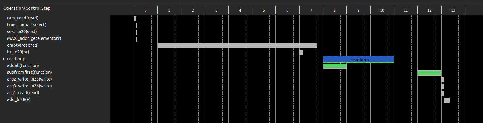
The design we have is OK, but it can be improved with directives. These tell HLS how to synthesise your software into hardware. First, let’s have a closer look at how your design is being implemented. In the Flow panel click C Synthesis -> Reports -> Schedule Viewer.
Info
If at this point your application complains about a lack of licence, obtain a free one as described on this page.
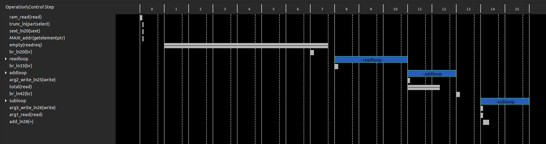
The rows are operations that come from your compiled code. The columns are states, and so looking vertically shows all the things that are happening in parallel. If two things are in the same column, they happen in parallel. Currently we can see that the addloop and subloop loops do not overlap, so they are not done in parallel. Note also that addloop and subloop have two states. This corresponds to the Performance Estimates we got from the synthesis report that told us the iteration latency of both these loops is two.
This is because I cheated. Sorry!
HLS would actually have done a better job, left to its own devices, but I included some directives in the code above to deliberately turn off some optimisations so that we could better see what they do. We will undo that in the next section. You can fully expand each loop to see the individual operations that take place in each state. You can also right click operations and select Goto Source to see the line of C++ code which created it, or the line of generated Verilog or VHDL that will create the actual FPGA hardware.
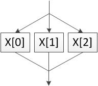
Pipelining loops
The first optimisation we will do is to tell HLS to pipeline addloop and subloop. They both have two states so they could be working on two elements of data at once. Without pipelining only one iteration will be running at a time, as shown in these diagrams.
| No pipelining | Pipelining |
|---|---|
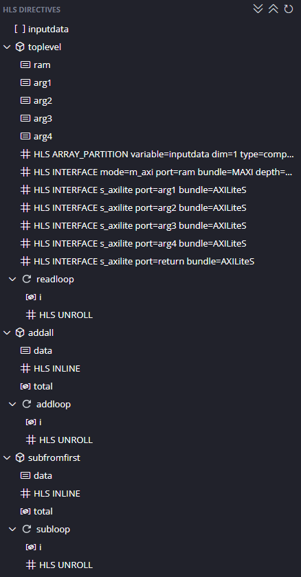
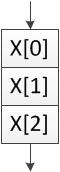 | 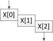 |
Go back to toplevel.cpp and select the HLS Directives button on the right (looks like two stars, or View → HLS Directives). This tab shows the items in the source file that you can attach directives to. Find addloop, and note that I included the directive HLS PIPELINE off. That tells it to not pipeline the loop. Double click that directive and in the dialog that pops up, uncheck off. Repeat for subloop.
Save the file and re-run synthesis (click the green arrow). Once it is done look at the report. Immediately we see that the latency of the design is now 512 cycles, down from 710 before. This is because the two loops are processing multiple data items at once.
In the synthesis report you will see the two loops are now pipelined, and if you expand the toplevel_Pipeline_addloop you will see that the loop it contains has an Interval of 1. This means a data item can be pushed into the loop each clock cycle. Their trip counts (number of times they execute) are 100 and 99, so their latencies are 100 and 99 cycles, down from the 200 and 198 of before.
Look back in the Schedule Viewer.
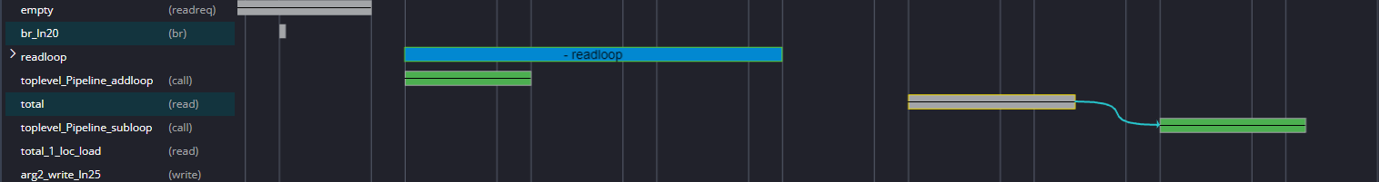
The green boxes are our pipelined loops. By clicking toplevel_Pipeline_subloop we see that it depends on total so a data dependency means that the two loops aren’t happening at the same time (they would be stacked on top of each other if they were). Instead, the speed boost comes from the fact that data items are pushed into the loops faster.
Unrolling loops
More drastic than pipelining loops is unrolling them. The UNROLL directive tells HLS to try to execute the individual iterations of the loop in parallel. This is very fast, but can cost a lot more hardware depending on the level of unrolling.
For toplevel.cpp click the x on the PIPELINE directives for the addloop and subloop loops to remove them. Click the + on the addloop loop in the Directive panel, select UNROLL.
Info
When adding a directive you can choose to put the directive in the source file (as an inline #pragma) or a separate config file. For our purposes it doesn’t matter.
We could add a factor here to limit the unrolling, but lets leave it blank to say to unroll as much as possible. Click OK and repeat for subloop. Resynthesise.
Now our design latency is down to around 420 cycles, meaning overall we are running at almost twice the speed of our original design. However we are now using around 7300 LUTs - we are over 3 times the size! HLS has also decided to use 4 Block RAMs for memory instead of 1 so that more data can be accessed in parallel. This is a classic time/space tradeoff.
Click on the Analysis perspective. Our design looks different again.
As we noted earlier, the hardware is completing the addall function before starting the subfromfirst function (one green box is after the other green box). Let’s force it to inline these functions so that it can schedule operations from both to happen together. Add the INLINE directive to the addall and the subfromfirst functions and resynthesise.
Now we are down to 366 cycles, and we’ve saved some hardware because HLS has been able to optimise across the two functions. We can still do better though!
Swapping Block RAMs for LUTs
Let’s tell HLS not to use Block RAMs and to instead just use normal registers. In some designs this can be very expensive, but it will allow true parallel access. Block RAMs are very storage efficient, but they can only support two things accessing them at any one time, and this is slowing us down. We can tell this by looking the Schedule Viewer and observing reads happening in pairs:
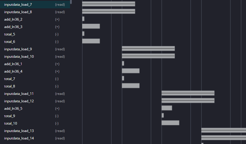
Now add a new directive to toplevel (near the top of the directives tab). Insert an ARRAY_PARTITION directive for variable inputdata of type complete.
Also, apply UNROLL to readloop as well, so we we can completely take advantage of the distributed RAM.
You should have the directives below. Resynthesise.
We now have a tiny design latency of only 115 cycles. Because the design reads in 100 data items we know our design will never be faster than 101 cycles so this is pretty good! Also notice we now our Block RAMs count has reduced and our LUT usage has increased again. Normally ARRAY_PARTITION will significantly increase LUT usage but increase parallelism and reduce BRAMs. This shows the importance of experimenting with directives, and using the Synthesis Report and Schedule Viewer to work out what is happening in parallel.
So we now have a very fast design, but we also know how to make it smaller (and slower) if we needed to by pipelining instead of unrolling.
Implementing it for real
We will work purely inside HLS using test benches for now. Later practicals will take HLS designs and connect them up to the ARM processing system.