Practical 1a - Getting Started
In this course you will be using a Xilinx Zynq-7000 FPGA on a Digilent Zybo Z7-10 board. The Zynq is a system-on-chip made from a combination of a dual-core ARM processor, an area of FPGA programmable logic, and various supporting peripherals.
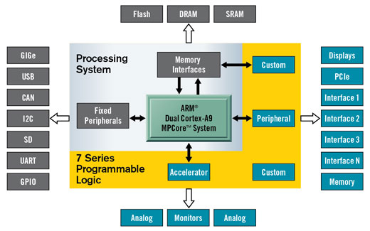
You will be creating software in C/C++ which runs on the ARM processors, and custom hardware accelerators which run in the programmable logic. Together, the Zynq can create complex systems for processing high volumes of data in a short amount of time. In these practicals we will learn how to do this stage by stage, starting with the ARM processors.
Task
We will learn how to create a project and start to get familiar with the interface. Today is just following the steps carefully - next week we will start to create our own designs. Go through this tutorial to make sure that you can get things working.
Important
Before you start, check that you have plenty of disk space or the tools will start behaving strangely.
Remote Access
Hopefully the majority of you will be able to work on this module in the Hardware Labs. However, it will be possible to work remotely. We have written detailed instructions for installing the Xilinx tools on your own computer. They are free to use for anyone with the type of FPGA that we have. Be warned that they are large and require at least ~60GB of free disk space (around 0.8 CoD Warzones, or 0.4 Baldur’s Gate 3).
Vivado
Vivado is the main software suite for creating Xilinx FPGA designs. It is installed at /opt/york/cs/net/xilinx_vivado-2025.1-x86_64-1/2025.1/Vivado/bin/vivado, which is a bit hard to remember, so you probably want to add that to your PATH.
echo 'export PATH=/opt/york/cs/net/xilinx_vivado-2025.1-x86_64-1/2025.1/Vivado/bin:$PATH' >> ~/.bashrcNow close and reopen your terminal and from then on you should be able to run Vivado with just vivado. Note that we are on version 2025.1, if you see it loading an older version like 2020 then something is wrong.
Important
Check you are running Vivado 2025.1 and not 2020. If you have loaded an older version, close and reopen your terminal so that the PATH we set up takes effect.
Creating a Project
Important
Warning
Never use spaces in the name or path of a Vivado project. This can cause issues later on.
- Open Vivado and select Create Project.
- Set a project name and location.
- Click Next and select “RTL Project” and “Do not specify sources at this time”.
- Click Next past adding Constraints as well.
- It will then ask you which FPGA you are building the project for. We need the Zybo Z7-10 from Vendor digilentinc.com.. If this is the first time you’ve worked in Vivado then digilent may not be in the list and you will need to click the “Refresh” button. It will pull all new board definitions (which takes a while) then it should be selectable.
- Set Vendor to
digilentinc.comand Name toZybo Z7-10. The status column will show a download icon. Click it to install the board definition. Once installed it will fill in the rest of the columns (I/O pin count, board rev, etc.) - Make sure
Zybo Z7-10is selected and click Next, then Finish.
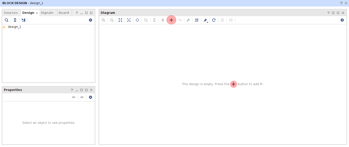
Creating a Block Design
We now have a project ready for the Zybo. To describe the hardware in the system we create a Block Design.
In the Flow Navigator window on the left-hand side of the main UI, select Create Block Design and click OK (using the default name is fine here, as you will generally have only one block design per Vivado project).
This creates a blank design, so we can now start adding “IP Cores”. IP Cores are pre-made components that can be used like Lego blocks to build a system quickly.
Adding the Zynq Processing System
The first IP we are going to add and configure the ARM processors, the memory interface, and other fixed peripherals on the SoC (together known as the Processing System or PS).
- Press one of the “Add IP” buttons, as shown in the screenshot below.
- Select from the list
ZYNQ7 Processing System. - After a good long think, your block diagram should be updated with a
Zynqblock. - The block represents the (fixed) ARM cores on the FPGA. Everything else we are about to add goes into the reconfigurable logic of the FPGA.
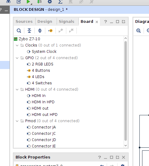
Adding LEDs and buttons
We want to connect to the buttons and LEDs on the board, so they can be controlled from code running on the ARM.
- Select
Boardfrom the centre top panel and you should see a list of the simple I/O on the board (see the screenshot below). - Double click
4 LEDsand click OK. Vivado will add a GPIO IP core which connects to the LEDs for you. - Double click
4 Buttonsand click OK. Vivado will also connect our IP core to the buttons.
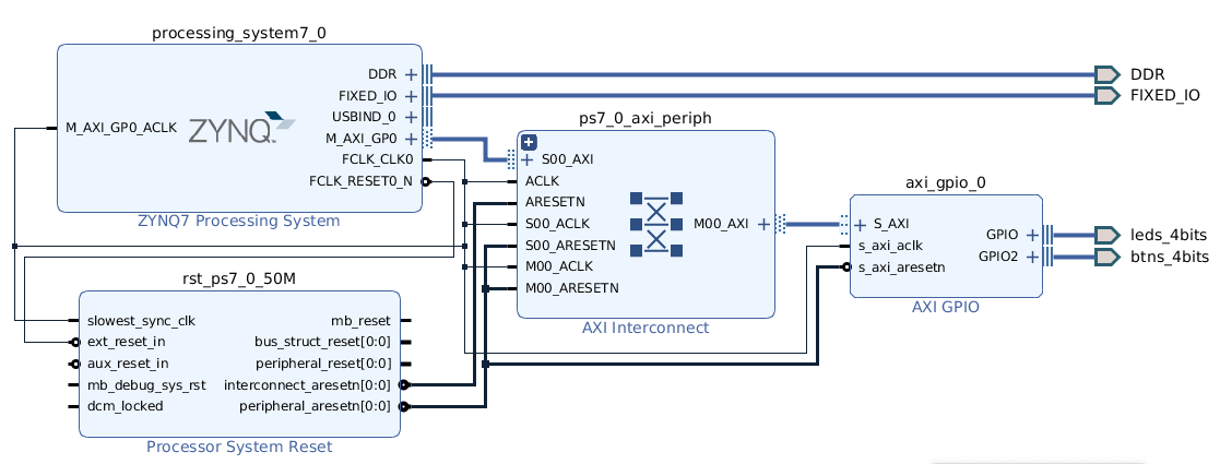
What did that do? We just created an instance of the axi_gpio core, which is a chunk of reconfigurable logic that allows general purpose IO (wires!) to be controlled from the main system bus (called the AXI bus). It is a very simple bit of logic. It just listens for bus transactions from the CPU. When written to by the CPU it sets the output wires, and when read by the CPU it reports the state of the wires.
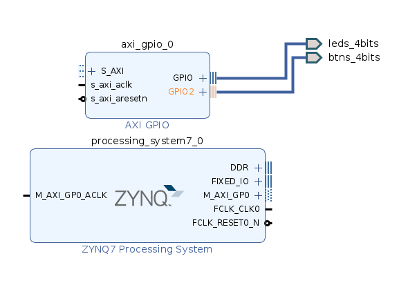
However, as you can see, while the GPIO core is in our design and is connected to the LED and Button inputs and outputs, it is not actually connected to the CPU (the Zynq block). We will address that now.
Vivado Designer Assistance
At this point, we have some IP blocks but they are not connected to each other. Fortunately, Vivado has noticed this and provides “Designer Assistance”.
- In the green prompt at the top of your design click “Run Connection Automation” and click OK.
Vivado will make some drastic looking changes to your design, but they are quite straightforward. It has done three things:
- Create and connect a “Processor System Reset”. This is an IP core which handles reset signals. Resets can be quite complex in an embedded system because different parts of the system run at different clock speeds. This core ensures that a stable reset signal is sent to the entire design. The tools will largely automate this.
- Create an AXI Interconnect. AXI is a system bus that allows the ARM processors to talk to other parts of the system. In this case, the GPIO core that we created. Again, the tools should largely handle this automatically.
- Connect the Processing System and the IO core to the AXI interconnect. AXI is a Master/Slave bus. Masters can initiate transactions, slaves can only reply to them. The Processing System’s general-purpose master AXI port (
M_AXI_GP0) and the GPIO core’s slave port (S_AXI) are connected together through the AXI Interconnect.
There should still be some Designer Assistance available because the Processing System block has some board-specific options which are not set up.
- Click “Run Block Automation” and click OK.
This makes less-visible changes, but is essential as it attaches DDR and other fixed I/O connections in the processing system to output pins on the FPGA device, and sets up internal parameters such as clock speeds.
Vivado has probably left everything looking a bit of a mess, so click the “Regenerate Layout” button in the toolbar to the top of the block diagram (third from right) to tidy up the layout. You can also manually drag the blocks around to improve the layout if needed.
Your design should now look something similar to this:
Create HDL Wrapper
We need to tell Vivado that our block design should be instantiated on the FPGA.
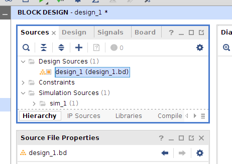
- Select Sources in the centre top panel.
- Right click your block design (
design_1.bd), and click “Create HDL Wrapper”. - On the next popup ensure “Let Vivado manage wrapper and auto-update” is selected and click OK.
A “critical warning” may appear with the following messages:
CRITICAL WARNING: [PSU-2] Parameter: PCW_UIPARAM_DDR_DQS_TO_CLK_DELAY_1 has negative value -0.044. PS DDR interfaces might fail when entering negative DQS skew values.
CRITICAL WARNING: [PSU-3] Parameter: PCW_UIPARAM_DDR_DQS_TO_CLK_DELAY_2 has negative value -0.035. PS DDR interfaces might fail when entering negative DQS skew values.
CRITICAL WARNING: [PSU-4] Parameter: PCW_UIPARAM_DDR_DQS_TO_CLK_DELAY_3 has negative value -0.100. PS DDR interfaces might fail when entering negative DQS skew values.
This is a known issue and can be ignored. However, any other “critical” warnings are likely to indicate a problem with your design.
Generate Bitstream
We are now ready to build the design.
- From the Flow Navigator on the left-hand side click Generate Bitstream.
Before the tools can create the bitstream (also called a bitfile) they will need to run synthesis and implementation on your design. It will prompt you about this if up-to-date results are not available, so click Yes to run the whole process. This will take a long time; welcome to FPGA development! For now this will only be a couple of minutes, but things can take much longer once your design gets more complicated. You can see progress by clicking the Design Runs tab at the bottom of the window. This will show you which stage is currently running and the elapsed time, but unfortunately not how long is remaining.
Synthesis and Implementation Reports
Once implementation is complete, select “Open Implemented Design” in the dialog box and click OK, or alternatively click “Open Implemented Design” in the Flow Navigator on the left. In future you can just click Cancel to this dialog box (or select any other option), but for now let’s inspect what the tools have done.
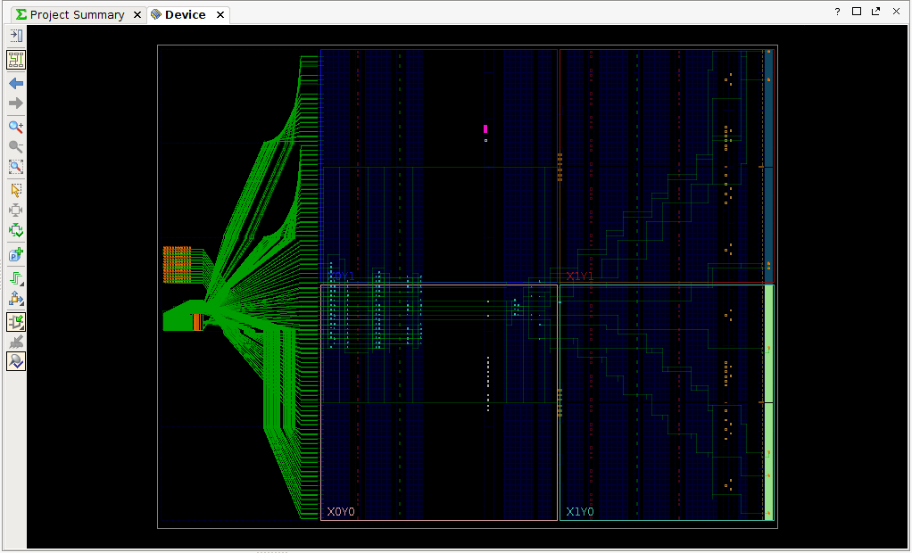
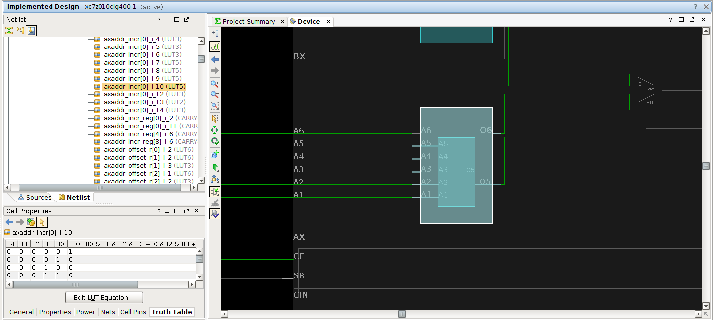
The Device view shows the layout of your design in terms of FPGA logic – the look-up tables (LUTs), multiplexors (MUXs), etc. that the device is made up of. The things on the left of the first image below are the ARM cores and external memory connections, and the parts inside the blue boxes show your (currently very small) design routed onto the FPGA logic
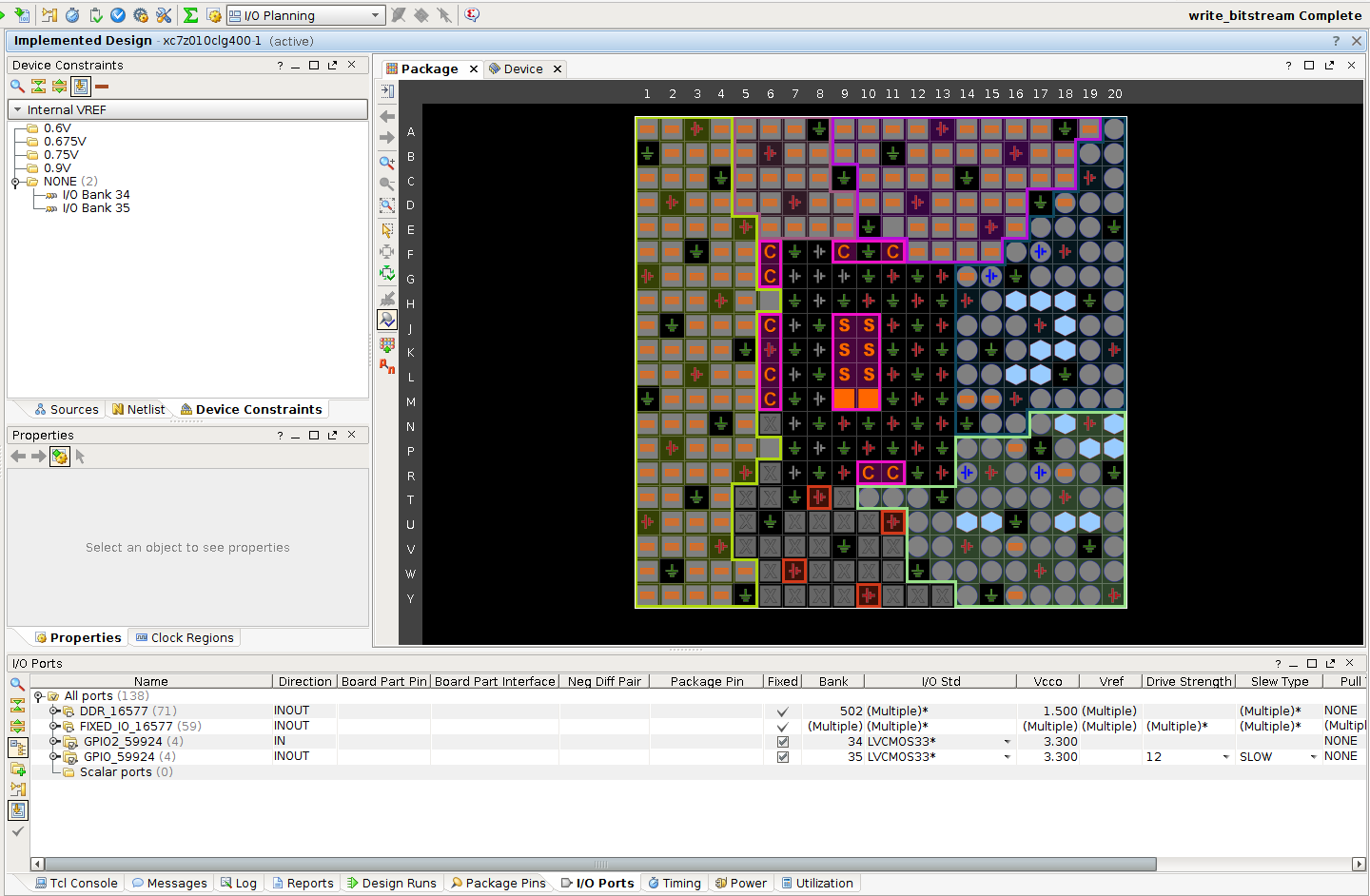
Click the “Routing Resources” button in the toolbar to also show the signals that are routed through the FPGA. From here, you can zoom in by dragging a box around components, and even inspect the truth tables of individual LUTs in the design. Have a look around to appreciate how the FPGA works. Changing “Default Layout” in the top right to “I/O Planning” allows you to see the physical pin assignments of the FPGA chip.
You can also view various reports (e.g. timing, power and utilisation) using the options in the flow navigator. This can be useful to see how much space your design is using on the FPGA fabric. Clicking “Report Utilization” brings up a summary of how your design fits on the device.
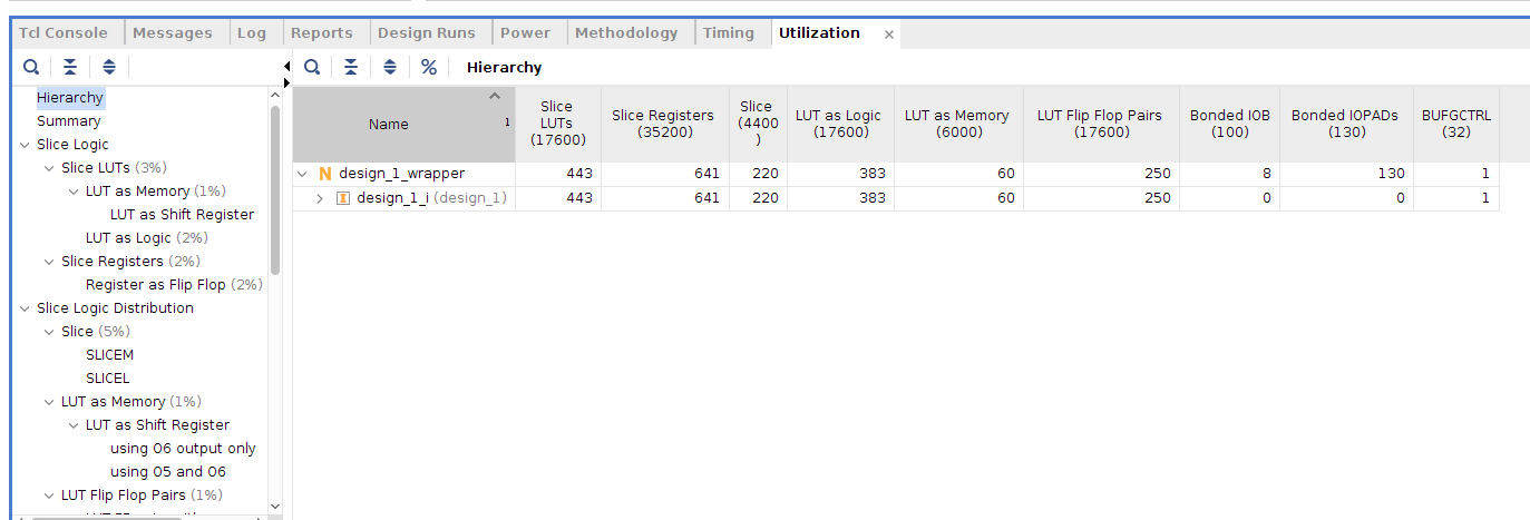
Whereas a software program only really consumes one resource, memory, FPGAs have many different resources. In the report you can see LUTs and Registers (a measure of logic space) and whether those LUTs are used to make logic or memory. If any of these numbers get larger than the number available on the device (shown in parentheses) then your design will not fit and the tools will error.
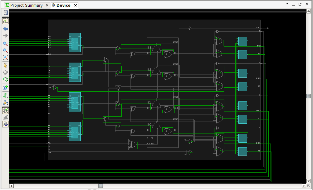
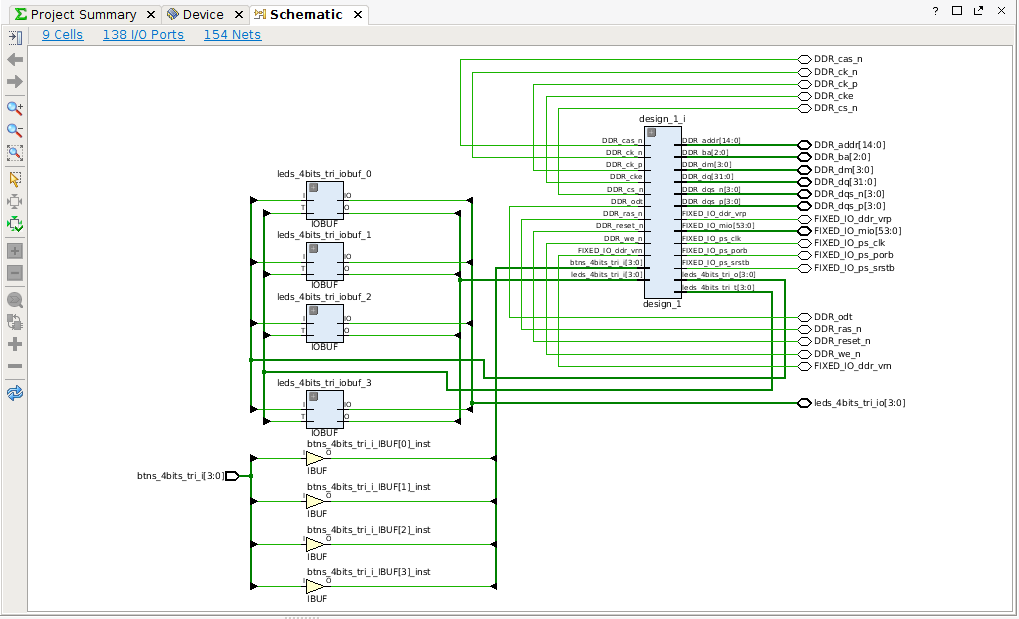
If you’re curious, you can also explore a logical schematic of your design as generated by the synthesis process, by choosing “Open Synthesized Design” then “Schematic” in the Flow Navigator.
Program the FPGA
Once you’ve finished having a look at implementation and synthesis output, we can program the FPGA with the generated bitstream.
At this point you should grab an FPGA board and connect it via USB to your computer. In the Flow Navigator click “Open Hardware Manager”, then “Open Target” and “Open New Target”. You should see following description of the connected FPGA:
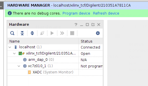
- To program the FPGA you can right click its part number (
xc7z010) and click Program Device, or use the green prompt at the top of the screen. - In the program dialog it should have selected the file
design_1_wrapper.bit(assuming you kept the name design_1 for your block diagram). - Click Program.
The programming should complete successfully (note the green DONE light on the FPGA board), but nothing will happen because the ARM cores have no software to make them do anything. Let’s write some!
Create a Software Project
To create software we need to use another application, Vitis IDE. Vitis’ job is to build software for the varying dynamic hardware architectures that we make in Vivado.
In Vivado select File -> Export -> Export Hardware. Select Next, “Include bitstream”, Next, and Finish. Then select Tools -> Launch Vitis IDE and click OK.
Info
For the last ~10 years, Vitis was built on top of Eclipse, but now it is built on top of Visual Studio Code. You are the lucky guinea pigs who get to try out their new IDE, and consequently encounter entirely new categories of bugs. We will go on this learning journey together.
Vitis has three types of project:
Platform
- This is what we just “exported”. It is a description of the design that you just built in Vivado, along with the bitfile that you just created.
- Contains low-level drivers to coordinate the boot up of CPUs, and descriptions of the IP cores in the system.
System
- Generated by the tools. Contains drivers, kernels, and frameworks that your applications can use. You can think of this as the Operating System, and is required by application projects.
Application Project
- Your code goes into application projects. These are built on top of a given System, for a given Platform.
First, we need to set the Vitis workspace. It may ask you on first launch, or if not, you can set it manually by selecting File -> Set Workspace. This should be a directory in your home directory, e.g. ~/vitis_workspace. It must not have spaces in the name. After setting, Vitis will relaunch and present you with an empty workspace.
First, we need to create a Platform project from the Vivado design which we just exported.
- Select File -> New Component -> Platform.
- Give it a name like
basicIO_platform, click Next. - Click
Browseand browse to what we exported from Vivado. If you didn’t change anything this will be in your Vivado project and calleddesign_1_wrapper.xsa. Click Next. - Vitis now reads our hardware design and will list compatible OS and processor choices. The defaults of
standalone(i.e. no OS) andps7_cortexa9_0are fine. Click Next and Finish.
Now that we have a Platform, we can create Applications that sit on top of it. You create your own applications through the File -> New Component -> Application menu but we are going to start with a “hello world” template.
- Select View -> Examples, and under
Embedded Software ExamplesselectHello World. ClickCreate Application Component From Template. - You can change its component name here from
hello_worldif you want, then click Next. - Select
basicIO_platformas the Platform, click Next. - Select
standalone_ps7_cortexa9_0, click Next and Finish.
We now have a Vitis project with a Platform and an example Application.
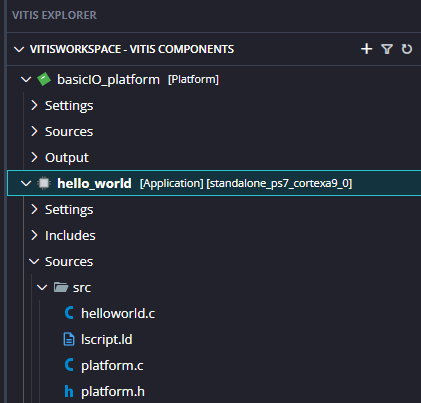
Expand hello_world and the src folder inside it, and double-click helloworld.c to see the example code SDK has created for you.
C or C++?
For the purpose of EMBS you can use either C or C++, the tools support both equally. However select C for this first application because C projects have a range of “hello world” templates to get you started, whereas C++ projects usually begin blank.
The EMBS documentation will mostly be in C, but you may use C++ if you wish. We would recommend that you do not rely on the very newest features of the language in case support hasn’t made it into the Xilinx tools yet. Whilst the compiler is standard GCC, the runtime is not standard glibc++ but a Xilinx-created embedded variant.
Flows
We are now going to build the project and then tell Vitis to send the compiled application to the FPGA to run. The Flow panel should be visible in the bottom left of the IDE. If not, click View -> Flow. Notice that the Component dropdown will show either basicIO_platform or hello_world to determine which project you are working on. Vitis will try to intelligently select the correct target for you based on which file you are looking at, but keep this target selector in mind.
Make sure you have selected the hello_world target and click Build. Vitis will understand that it also needs to build the platform. Once complete it will put a little green checkmark next to Build. Before we run it though we need to connect a serial terminal so that we can see the output. Make sure that the FPGA is connected and turned on, start a Terminal and run:
screen /dev/ttyUSB2 115200In this command, screen is a terminal application, and /dev/ttyUSB2 is the device that the FPGA appears as. Finally 115200 is the baud rate to communicate at. If this works, you will get a blank window. To exit screen press Ctrl-a, release all keys, then press k (or just turn off the FPGA).
“Help! Screen says file not found!”
Sometimes the serial devices enumerate in the opposite order so sometimes you will have to experiment with another device node, such as:
screen /dev/ttyUSB1 115200
With screen running, click Run. After a short time, “Hello World” should appear in the screen terminal that you opened earlier. Note, this is not the Console in Vitis.
Task
Change the software to print a different string, rebuild, and relaunch. You should see the printed string change. Note that you have to remember to rebuild your software!
Once you have the hang of the tools, and have successfully programmed the FPGA and run some software you are done for our first session!